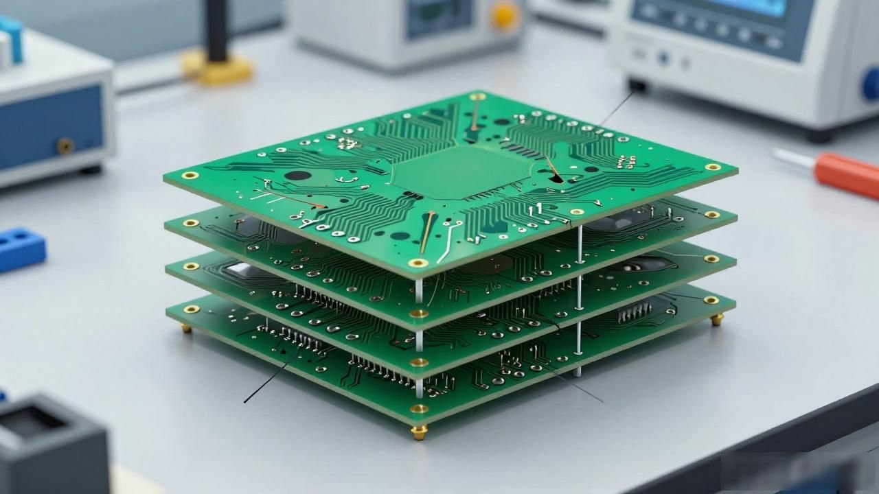


A method for manufacturing a multi-layer circuit board double-sided riveted structure
Pain points of traditional crafts
When producing multi-layer circuit boards, the most troublesome part is the lamination process. The traditional method can easily distort the board and cause the internal circuits to break. Once a nail breaks, the entire batch of products will be scrapped, causing huge losses. This will not only cause a waste of materials, but also slow down the delivery speed, thereby severely compressing the factory's profits.
What workers face every day is an astonishingly high scrap rate and a pitifully low yield rate. In order to pursue high precision, they often sacrifice output. This contradiction makes management anxious. How to improve efficiency while ensuring quality has become a real problem that the industry urgently needs to solve.
Riveted structural design
The new structure limits the length of the rivets to 65% to 75% of the plate thickness. This ratio has been accurately calculated and can not only fix the laminates but also prevent them from penetrating the surface. The rivets are designed with solid rods, which are stronger and less prone to deformation. Such optimization of details directly improves the reliability of the connection.
The hole was redesigned into an elliptical shape with an aspect ratio ranging from 2.0 to 2.5. It is a positioning hole. Scale marks are added next to it so that workers can quickly align. The horizontal and vertical holes are alternately distributed to ensure uniform force. These changes may seem small, but in fact they greatly reduce the difficulty of operation.
Alternate riveting on both sides

The key difficulty lies in the multi-layer multi-pass riveting technology of thick plates , which uses rivets that alternately rivet in forward and reverse directions. This shows that the force directions of each layer cancel each other out. This balance mechanism effectively prevents the plate from warping under high pressure and high temperature. The problem of distortion and deformation that is originally very easy to occur has been fundamentally solved.
Four sets of rivet holes evenly distributed on the edge provide a stable support point. There are four holes on each side. It is a manufacturing method of double-sided riveted structure of multi-layer circuit boards. The symmetrical layout makes the pressure dispersion more reasonable. Such a design is particularly suitable for thick plate multi-layer structure and thick plate multi-layer multi-pass riveting technology , ensuring the stability and consistency of the overall structure and reducing stress concentration.
Improve production efficiency
The original preparation process before lamination has been simplified by the new process. This is due to the fact that the scale points and elliptical holes can provide intuitive guidance, so that workers do not have to repeatedly adjust the positioning, and the installation speed is significantly accelerated. The processing time of a single board is shortened, which results in a much higher output in the same time.
Reducing the rework rate is a very important step in improving efficiency. Since the problems of broken nails and deformation have been effectively controlled, the one-time pass rate has been greatly improved. The factory no longer needs to consume a lot of manpower to repair defective products, and its resources can be focused on producing more qualified products. The overall efficiency has shown a trend of significant growth.
Quality Control Advantages
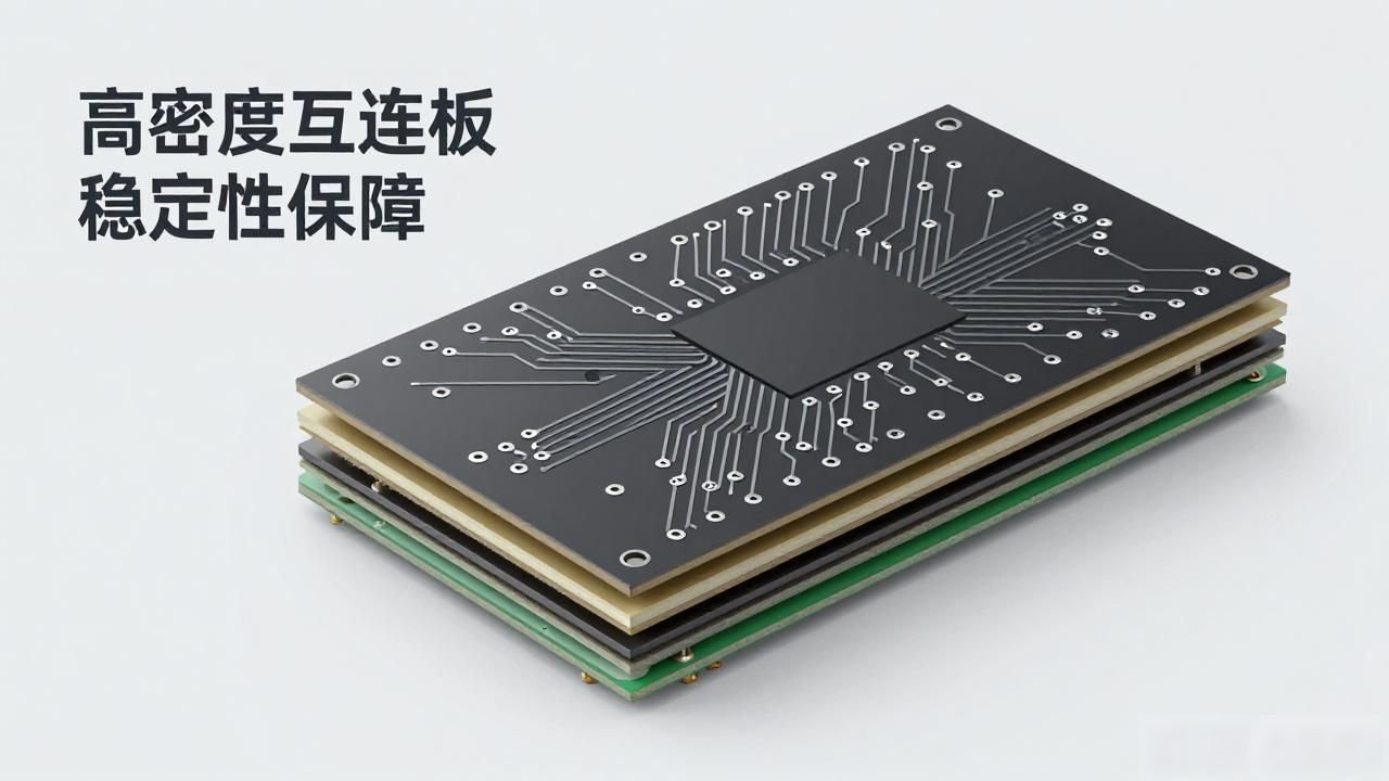
The interlayer bonding force is enhanced by the double-layer riveted structure. During subsequent processing, the circuit board becomes more stable and less likely to become loose. This is extremely important for high-density interconnect boards, because even extremely small displacements may cause circuit failure. This structure guarantees the stability of electrical connections at the physical level.
There is a certain space for thermal expansion and contraction that is allowed by the oval positioning holes. During the high-temperature lamination process, the plate will deform slightly, and the positioning holes can absorb these stresses. After cooling, the plate returns to a flat state, and the dimensional accuracy is maintained at a high level, meeting the stringent requirements of high-end electronic products.
Industry application prospects
This technology is particularly suitable for areas with extremely high reliability requirements, such as aerospace and medical equipment. These industries cannot tolerate the serious consequences of circuit board failure. The double-sided riveted structure provides higher safety and becomes one of the preferred solutions for high-end manufacturing.
As electronic products evolve towards thinner, lighter and higher density, the demand for multilayer boards will continue to increase. This technology resolves long-standing quality control problems by optimizing structure and process. It not only improves product performance, but also brings considerable economic benefits to manufacturers, and is truly worthy of widespread promotion.
Do you think this double-sided riveting technology can further reduce costs when using thick plate multi-layer multi-pass riveting technology in the mass production of smart home equipment? You are welcome to leave a message to share your views. If you think it is useful, please like it and forward it to more peers.






暂无评论内容